Custom Chips
Section Incomplete
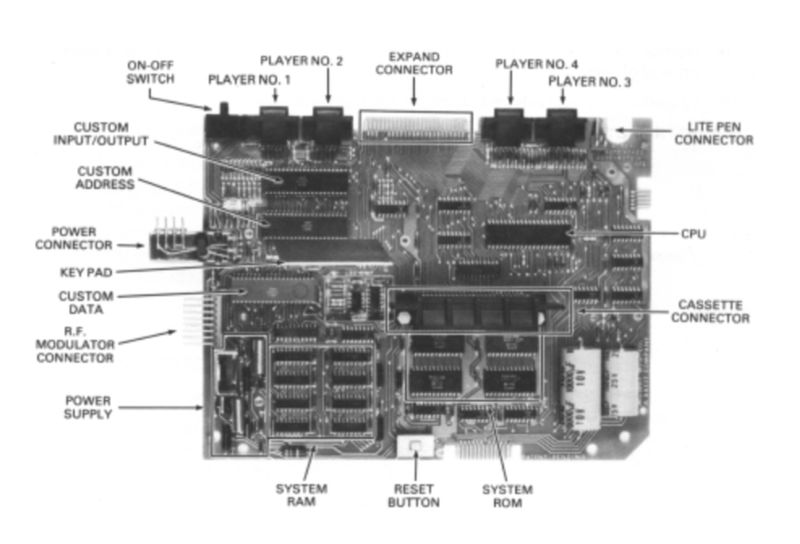
System Board
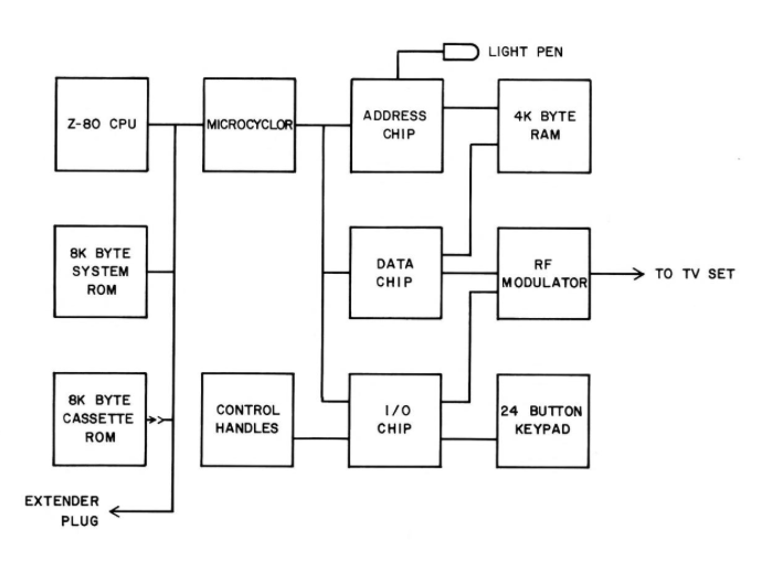
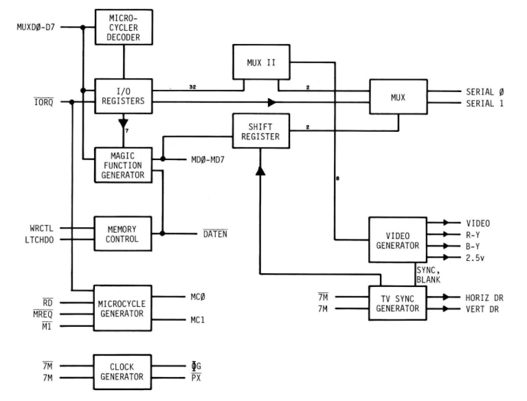
System Block Diagram
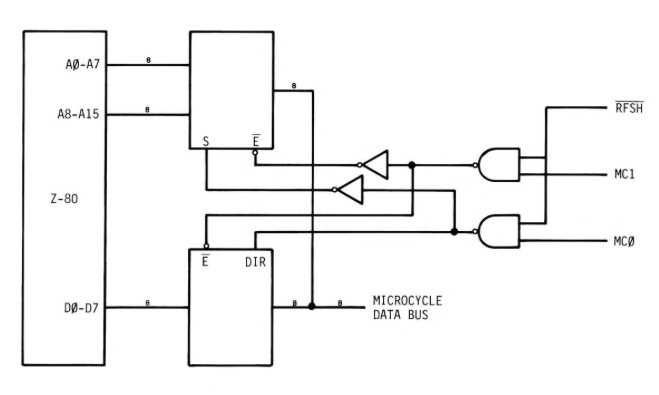
Microcycler
The purpose of the microcycler is to combine the 16-bit Address Bus and the 8-bit Data Bus from the Z80 into one 8-bit Microcycle Data Bus to the Data Chip, Address Chip, and I/O Chip. This was done to reduce the pin count on the custom chips.
The Microcycle Data Bus can be in any of four modes. Its mode is controlled by MC0 and MC1 coming from the Data Chip and RFSH (high) from the Z80. The modes are as follows:
| RFSH (high) | MC0 | MC1 | Microcycle Data Bus Contents |
|---|---|---|---|
| 0 | 0 | 0 | A0–A7 from Z80 |
| 0 | 0 | 1 | A0–A7 from Z80 |
| 0 | 1 | 0 | A0–A7 from Z80 |
| 0 | 1 | 1 | A0–A7 from Z80 |
| 1 | 0 | 0 | A0–A7 from Z80 |
| 1 | 0 | 1 | A8–A15 from Z80 |
| 1 | 1 | 0 | D0–D7 from Z80 |
| 1 | 1 | 1 | D0–D7 to Z80 |
MC0 and MC1 change 140 nsec after the rising edge of Φ. Their changes are shown in the timing diagrams of various instruction cycles.
[NM:110]
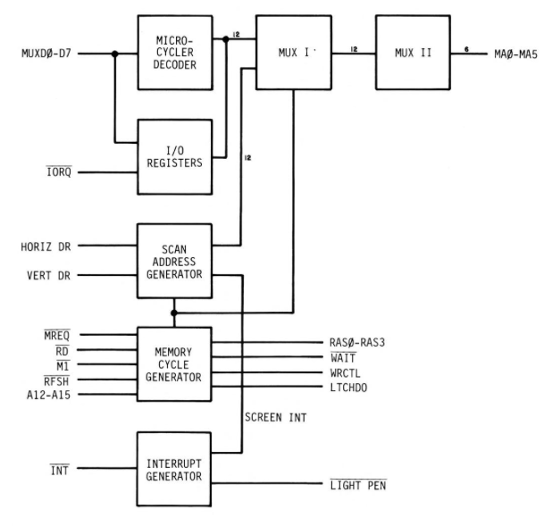
Address Chip
Data Chip
I/O Chip
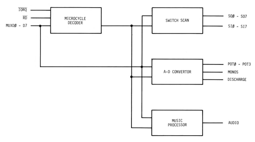
The Z80 communicates with the I/O Chip through input and output instructions. The state of an 8×8 switch matrix can be read through the Switch Scan circuit. When an input instruction is executed, one of the SO0–SO7 lines will be activated. When a line is activated, the switch matrix will feed back eight bits of data on SI0–SI7. This data is in turn fed to the Z80 through MUXD0–MUXD7.
The Z80 can read the position of four potentiometers (pots) through the A-D Converter circuit. The pots are continuously scanned by the A-D Converter, and the results of the conversions are stored in a RAM in the A-D Converter circuit. The Z80 simply reads this RAM with input instructions.
The Z80 loads data into the Music Processor with output instructions. This data determines the characteristics of the audio that is generated.
